The PCB Trace Placement and Return Inductance
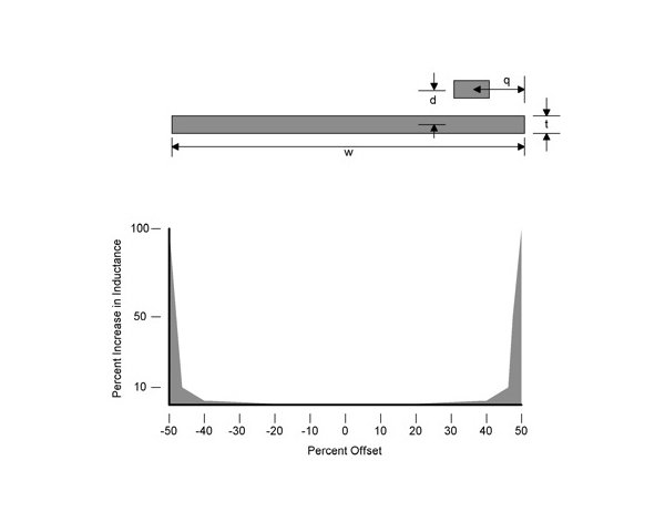
As a signal trace is moved towards the edges of a return plane, the inductance of the return plane rises causing more radiation. Placement near the edge of the board allows more flux from the signal trace to wrap around the return plane increasing its inductance. The result can be dramatically increased electromagnetic emissions (EMI) and reduced electromagnetic compatibility (EMC). From “Know the Theory of Partial Inductance to Control Emissions.”